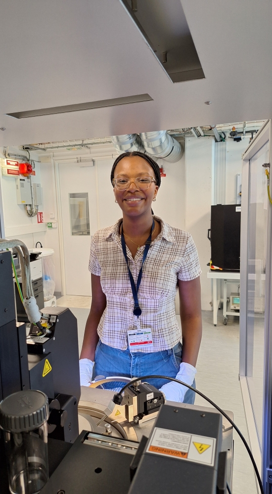
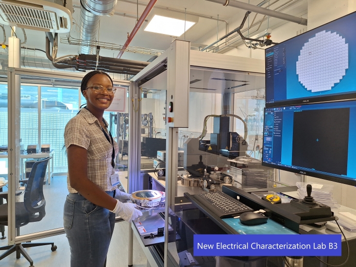
"My project focused on supporting the implementation of stress testing to study and model voltage-induced polarization domain reversal in LTO wafer layers. I contributed by developing a procedure for a systematic stress test and collecting data under a variety of conditions. Also, I gained hands-on experience with new equipment, such as the Atomic Force Microscope (AFM). I also learned to navigate the realities of working in industry, where progress often depends on others’ availability."

Zuri's story
MechE major Zuri '27 interned at a semiconductor materials manufacturer in France during the summer of 2025. The experience in a corporate setting provided the exposure that she needed to support her academic and career goals. This reinforces her interest to pursue a career in engineering and medicine.
"I gained a better understanding of the real-world challenges of industry research, such as equipment availability, dependence on cross-functional teams, and working on problems that do not yet have established solutions. These lessons reinforced my interest in pursuing a career at the intersection of engineering and medicine."Zuri Vallery '27
Major and Class Year
Mechanical Engineering (2), Class of 2027
MISTI program
Internship
Location
France
Host
SOITEC SA